
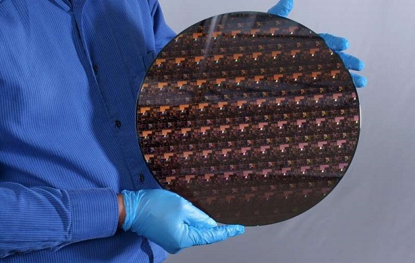
(*2*)IBM has unveiled a breakthrough in semiconductor design and course of with the event of the
(*2*)world’s first chip with 2 nanometer (nm) nanosheet know-how. Semiconductors play crucial roles in every little thing from computing, to home equipment, to communication units, transportation programs, and demanding infrastructure.
Demand for elevated chip efficiency and power effectivity continues to rise, particularly within the period of hybrid cloud, AI, and the Web of Issues. IBM’s new 2 nm chip know-how helps advance the state-of-the-art within the semiconductor business, addressing this rising demand. It’s projected to attain 45 % larger efficiency, or 75 % decrease power use, than in the present day’s most superior 7 nm node chips.
The potential advantages of those superior 2 nm chips may embody:
- Quadrupling cellphone battery life, solely requiring customers to cost their units each 4 days.
- Slashing the carbon footprint of information facilities, which account for one % of worldwide power use. Altering all of their servers to 2 nm-based processors may doubtlessly cut back that quantity considerably.
- Drastically dashing up a laptop computer’s features, starting from faster processing in purposes, to aiding in language translation extra simply, to sooner web entry.
- Contributing to sooner object detection and response time in autonomous autos like self-driving vehicles.
“The IBM innovation mirrored on this new 2 nm chip is important to all the semiconductor and IT business,” stated Darío Gil, SVP and Director of IBM Analysis. “It’s the product of IBM’s method of taking over laborious tech challenges and a demonstration of how breakthroughs may end up from sustained investments and a collaborative R&D ecosystem method.”
This newest breakthrough builds on a long time of IBM management in semiconductor innovation. The corporate’s semiconductor growth efforts are primarily based at its analysis lab situated on the Albany Nanotech Complicated in Albany, NY, the place IBM scientists work in shut collaboration with private and non-private sector companions to push the boundaries of logic scaling and semiconductor capabilities.
IBM’s legacy of semiconductor breakthroughs additionally contains the first implementation of seven nm and 5 nm course of applied sciences, single cell DRAM, the Dennard Scaling Legal guidelines, chemically amplified photoresists, copper interconnect wiring, Silicon on Insulator know-how, multi core microprocessors, Excessive-k gate dielectrics, embedded DRAM, and 3D chip stacking. IBM’s first commercialized providing together with IBM Analysis 7 nm developments will debut later this 12 months in IBM POWER10-based IBM Energy Techniques.
50 billion transistors on a fingernail-sized chip
Growing the variety of transistors per chip could make them smaller, sooner, extra dependable, and extra environment friendly. The 2 nm design demonstrates the superior scaling of semiconductors utilizing IBM’s nanosheet know-how. Its structure is an business first. Developed lower than 4 years after IBM introduced its milestone 5 nm design, this newest breakthrough will permit the 2 nm chip to suit as much as 50 billion transistors on a chip the dimensions of a fingernail.
Extra transistors on a chip additionally means processor designers have extra choices to infuse core-level improvements to enhance capabilities for forefront workloads like AI and cloud computing, in addition to new pathways for hardware-enforced safety and encryption. IBM is already implementing different modern core-level enhancements within the newest generations of IBM {hardware}, like IBM POWER10 and IBM z15.
Supply:https://www.ibm.com/tr-tr
IBM unveils world’s first 2 nanometer chip know-how, opening a new frontier for semiconductors
(*2*)Scientists unveil newest femtosecond laser
Dikkat: Sitemiz herkese açık bir platform olduğundan, çox fazla kişi paylaşım yapmaktadır. Sitenizden izinsiz paylaşım yapılması durumunda iletişim bölümünden bildirmeniz yeterlidir.
Supply: https://www.bizsiziz.com/ibm-unveils-worlds-first-2-nanometer-chip-technology-opening-a-new-frontier-for-semiconductors/

